Recently, scientists of the University of Stuttgart in collaboration with research groups of the University of Duisburg-Essen and the Technion in Haifa successfully demonstrated this extreme light compression experimentally. Furthermore, they were able to take slow motion movies with steps of less than one femtosecond between single images that enable the experimental observation of wave propagation and formation of a nano-focus of only 60 nanometers diameter for 800 nanometer excitation wavelength.
Light is characterized by its frequency and its wavelength. The frequency indicates how often the electromagnetic field oscillates within one second. The wavelength, which is between 400 and 800 nanometers (one millionth of a millimeter) for visible light, specifies the distance between two wave maxima.
Usually, frequency and wavelength are connected directly with each other, because their product is just the velocity of light in vacuum.
On metal surfaces however, this relation can be altered. Such material interfaces allow the excitation of surface plasmons due to freely oscillating electrons. These surface electron waves exhibit a substantial wavelength shortening compared with the incident light. More detailed investigations show that the electric field of the light excites motion of the electrons at the surface and concentrate them in areas of high and low electron density. This resembles waves on water surface.
In water, the distance between waves is dependent on its depth. This effect also holds for metal surfaces. One just has to vary the metal thickness in a suitable way. It turns out that for metal films of about 20 nanometers thickness, which are deposited on a silicon surface, the wavelength of visible light can be squeezed by a factor of 5 or more.
So far, this theoretically predicted effect was difficult to observe in experiments and is far from technical applications. The reason for this is that ultra-smooth high quality metal films are difficult to fabricate. Smallest metal grains and crystallites formatting on the surface during evaporation influence wave propagation on smooth surfaces due to their roughness.

Recently, scientists of the University of Stuttgart in collaboration with research groups of the University of Duisburg-Essen and the Technion in Haifa successfully demonstrated this extreme light compression experimentally. Furthermore, they were able to take slow motion movies with steps of less than one femtosecond between single images that enable the experimental observation of wave propagation and formation of a nano-focus of only 60 nanometers diameter for 800 nanometer excitation wavelength. This nano-focus is smaller than one tenth of the light wavelength while commonly only half of the excitation wavelength can be reached.
Key of this experiment was the discovery of a new method to fabricate atomically flat, several micrometers large and single crystalline gold surfaces of adjustable thickness on ultra-smooth silicon surfaces. These gold films of ultimate surface quality were the precondition to observe surface plasmon waves with femtosecond laser pulses and a modified electron microscope in a so-called PEEM-experiment. PEEM stands for Photoelectron Emission Microscopy.
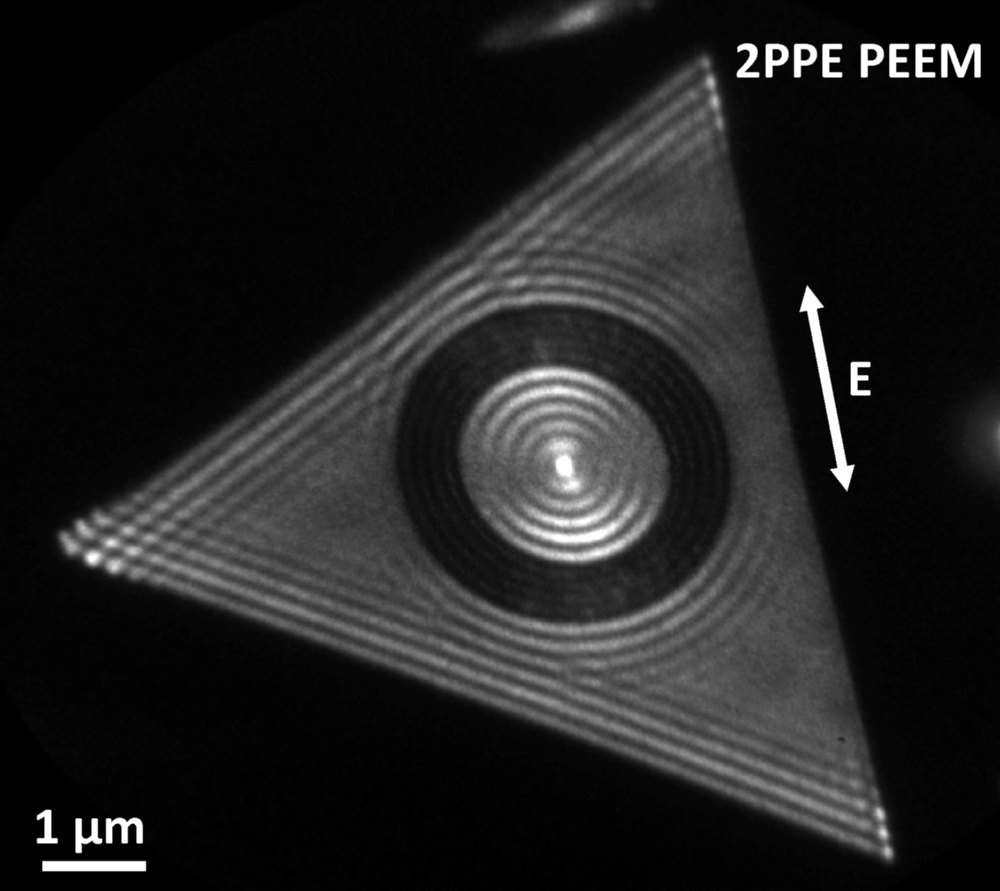
These laser pulses impinge on edges of the gold films and on specific circular line grids where they are transformed into surface plasmons. The fact that these gold films are atomically smooth on both sides allows antisymmetric and symmetric coupling of the two surface waves. Therefore, formation of long- as well as short-range surface plasmon takes place. The latter one exhibits the extremely reduced wavelength.
For laser pulses of sufficient energy, two photons of the laser beam transfer enough energy to electrons inside the gold that allow electron emission from the surface. At surface plasmon maxima, there is extremely high energy density and electrons can escape from the surface. These electrons can be imaged with an electron microscope. Using two subsequent laser pulses of increasing time delay, entire movies of plasmon waves can be generated.
This new method is ideal to produce extremely small focal spots that emit a large amount of electrons within short time periods. Possible applications include imaging with higher spatial resolution, nonlinear microscopy, nonlinear exposure of photoresists in the near field, heat-assisted magnetic data storage, as well as electron microscopy with highest temporal and spatial resolution.
Expert Contact:
Prof. Dr. Harald Giessen, Dr. Bettina Frank, University of Stuttgart, 4th Physics Institute, Tel. +49 711 6856 -5111, -5109, EMail: giessen@physik.uni-stuttgart.de, b.frank@pi4.uni-stuttgart.de
Reference:
B. Frank, P. Kahl, D. Podbiel, G. Spektor, M. Orenstein, L. Fu, T. Weiss, M. Horn-von Hoegen, T. J. Davis, F.-J. Meyer zu Heringdorf, and H. Giessen: Short-range Surface Plasmonics: Localized Electron Emission Dynamics from a 60 nm Spot on Atomically Flat Single Crystalline Gold. Science Advances 3, e1700721 (2017),