Internet, payments, electricity, traffic: nothing can dispense with integrated circuits these days. Due to the omnipresence of chips and computers, semiconductor tests are also becoming increasingly important. The University of Stuttgart is establishing a graduate school in close collaboration with Advantest to promote early career researchers and research in this field.
The products of the 480 billion US dollar semiconductor industry are paving the way for new or improved functions in more and more everyday products. “In fact, contemporary societies depend on chips functioning reliably and securely,” says Prof. Hans-Joachim Wunderlich, head of the Chair of Computer Architecture at the Institute of Computer Architecture and Computer Engineering (ITI) at the University of Stuttgart. “Without regular checks, the reliability and security of the chips cannot be guaranteed,” says Wunderlich. “This is why the tests also cover the entire life cycle of an integrated circuit from development to production to operational monitoring.”
Early detection reduces costs
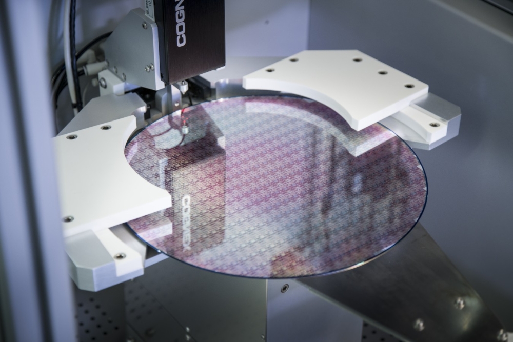
Developers who design a new chip can use increasingly precise mathematical models for this purpose. But at the same time, the miniaturization of structures and the increase in complexity are progressing equally rapidly. By itself, the order of magnitude involved, which is in the range of a few nanometers, makes it difficult to accurately predict the behavior of the new chip. “Tests on prototypes therefore already contribute to better development results in this early phase,” says Wunderlich. When the chip goes into production, the manufacturing process is successively optimized. The result is that at the beginning of the process, many chips land in the wafer reject bin, i.e., don’t meet the strict requirements specified for them. Therefore, the initial yield is often only a few percent. “The purpose of test runs performed here is, on the one hand, to separate the wheat from the chaff and, on the other hand, to derive important findings from the measurement data which could improve the production process,” explains Wunderlich. “In this way, the manufacturer gradually manages to increase the yield per wafer thus reducing unit costs.” Manufacturers are aiming for mass production yields of 99 percent for memory chips, such as those found in every PC and smartphone.
But even when an integrated circuit has left the factory and is working in a computer system, no matter which kind, testing continues to play a role. “Instruments are integrated on the chip that monitor the work of the other circuits,” says Wunderlich. “On the basis of the test data obtained, the manufacturer can analyze a return after a failure in order, at best, to adapt the development or manufacturing process accordingly.” And so to avoid the problem in the future.
Experts wanted
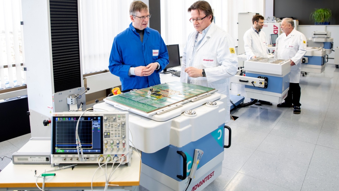
What sounds very complicated to the layman represents a veritable pool of options for experts. “When testing chips, you acquire data about how several hundred parameters change over time, many of which are interdependent,” says Wunderlich, outlining the challenge. Such parameters could include such things as temperatures, voltages, currents or the susceptibility of a signal to interference. “This data is difficult to interpret,” says the scientist, because it is often the case that only a handful of the parameters play a role in the effect under investigation. Finding them is like the infamous search for a needle in a haystack, a search that also requires a great deal of expertise. The University of Stuttgart’s Faculty Five is, therefore, planning to conduct research into such issues in the new graduate school in collaboration with Advantest, a Tokyo-based company, whose second largest site is located in Böblingen and is one of the leading suppliers of automated test solutions and measuring instruments for the semiconductor industry. They will be providing the funding for equipment, jobs and the qualification program and providing each doctoral student with a mentor. A stay abroad is also planned.
Instruments are integrated on the chip that monitor the work of the other circuits.
Prof. Hans-Joachim Wunderlich
Research using real data
“We have been working with Professor Wunderlich’s team and other university teams on a caseby- case basis for decades,” says Klaus Siegert, Vice President of Research & Development at Advantest in Böblingen. “But the graduate school is a new dimension.” The company's medium-term strategy is to build a cloud-based test infrastructure for its own customers based on data and artificial intelligence. Collaborations, such as those with the University of Stuttgart, will also contribute to this. “The German site is the first to have initiated such a close collaboration,” says Siegert. The collaboration is initially scheduled to run for six years, but an extension is not excluded. Neither partner will apply for patents for anything based on their joint research. In this way, they will ensure that neither publications nor the commercialization of results will be prevented. “The graduate school offers the opportunity to work with real data on something that will meet with great interest in industry,” promises Siegert, who studied electrical engineering at the University of Stuttgart 28 years ago.

AI on the testbench
Artificial Intelligence (AI) will also be important for the work carried out by the Research Training Group, partly in connection with the methodologies used to deal with specific questions, but also for when it comes to identifying the correct parameters for a given problem. “It is important to note that - unlike in many other industries in which AI methods are used - semiconductor testing does not depend solely on classification,” Wunderlich emphasizes. “Instead, it's always about understanding why certain interdependencies occur.” The relevant development and manufacturing process or operation cannot be optimized without this understanding.
In addition to the search for causes of design and product issues, the scientist sees four further fields in which AI could be useful in testing, for example, in connection with methods that help to better understand confusing test data, and for configuring the best working states of a particular chip. “Predicting lifetime and maintenance requirements is also a task that could be handled by AI,” says Wunderlich. And finally, AI will help with designing tests as efficiently and effectively as possible. “Adaptive tests - those that learn from their own results - are our vision.”
Michael Vogel
Prof. Dr. Hans-Joachim Wunderlich
Institute of Computer Architecture and Computer Engineering (ITI), University of Stuttgart.