Table of Content
Further information:
Atom probe tomography (APT) is an outstanding microscopy technique capable of revealing materials composition with sub-nanometer spatial resolution and single-atom chemical sensitivity. Processing of the measured data results in detailed 3D maps of the analyzed volume.
Competence Center
The Stuttgart group has extensive long-term experience in the field of atom probe tomography. As one of only a few groups in the world, we develop, build, and operate our own custom-made instruments and tools for the software-based data analysis. APT is key in many of our research projects. A modern FIB and a HR-TEM in the lab enable state-of-the-art sample preparation and correlative microscopy.
Operation Principle
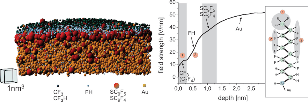
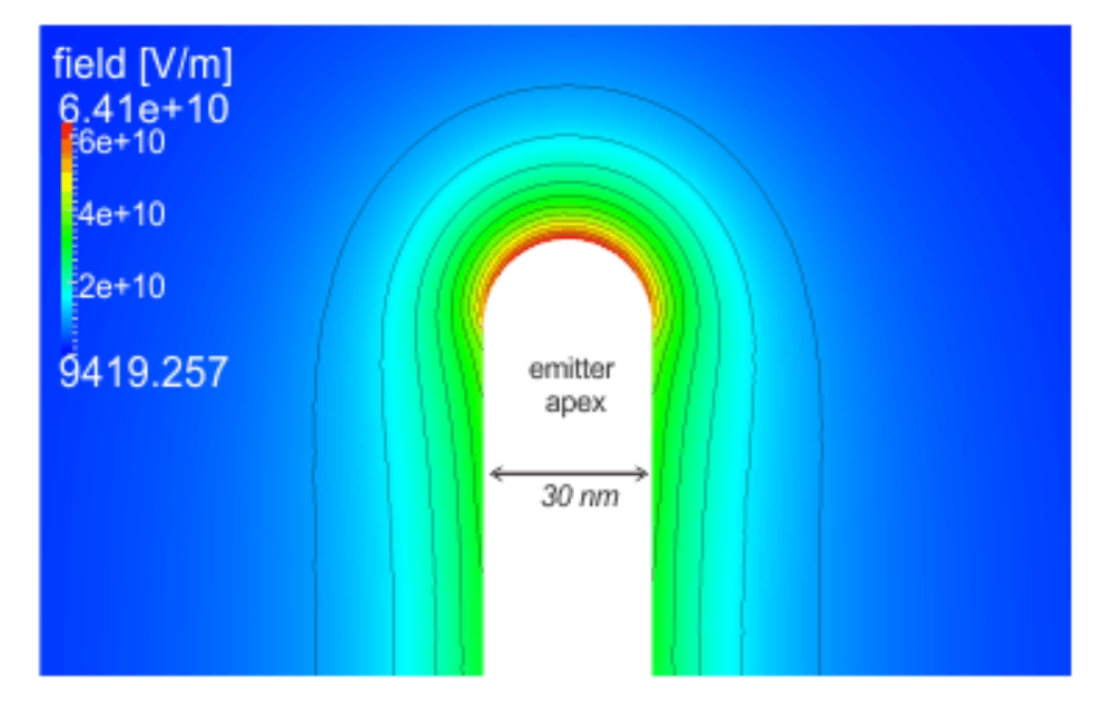
Analyzed samples in APT are needle-shaped tips. Owing to this particular geometry, an extraordinary high electric field in the order of 1010 V/m develops, if the samples are subjected to a moderate high-voltage. This field is sufficient to ionize protruding surface atoms, e.g. those located at the terrace edges or at kink sites. This so called field evaporation can be precisely controlled by the voltage applied to the specimen to obtain a continues evaporation of the sample in an atom-by-atom manner.
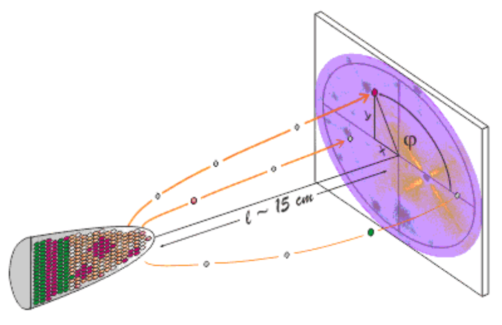
Core aspects of the technique are the controlled erosion of atoms at the nanoscale, their measurement by means of a two-dimensional position-sensitive detector system and their identification based on time-of-flight mass spectrometry.
Eventually, a 3D computer model of the destructed sample is reconstructed by processing the recorded ion hits taking into account the sequence of detection events and evaluating the trajectories by a transparent point projection law.

Method of choice for nanoscale materials analysis
In recent years, APT gained increasing attention. The introduction of laser-asssisted atom probe instruments decisively extends the class of applicable materials, from well conducting metals to semiconducting and insulating materials. APT is going to become an indispensible tool in modern materials science. Related research includes but is not limited to
- solid state reactions (diffusion, precipitation, phase transformation)
- characterization of complex nanostructures (e.g. semiconductor circuits, nano-compounds)
- bio-materials and soft-matter (self-assembled monolayers, polymers)